We have an excellent technical team, our products in quality and quantity will make you satisfied, welcome to buy
Views: 19 Author: Site Editor Publish Time: 2018-03-13 Origin: Site
In the past five years, the contribution rate of China's scientific and technological progress to GDP has increased from 52.2% in 2012 to 57.5%, and the global ranking of national innovation capacity has risen from 20th to 17th. Mechanisms, talents, and finances, like finely-woven neural networks and blood vessels, continue to nourish China’s steel bars and bones. This is another important device for the manufacture of China’s heavy equipment—a unique fertile ground for China’s system, which is gathering together Lasting, deepest innovation.
Blue Whale One, Sky Eye, large aircraft, domestic aircraft carrier, one of the world's most powerful devices, made people proud and praised the world. Behind these world-renowned achievements, both reflect the unique advantages of China's efforts to concentrate on major issues. In the report, CCTV also specifically mentioned a heavy device used for the manufacture of large-scale integrated circuits: ultra-high-purity metal sputtering targets.
Ultra-high-purity metal sputtering target is a necessary equipment for chip manufacturing. It is mainly used for manufacturing 300mm ultra-large-scale integrated circuits. Its material purity is required to be more than 99.999%. This also involves the application of tungsten. In view of this, Xiaobian solemnly Tell us about today's protagonist, the tungsten target.
Sputtering is one of the main technologies for the preparation of thin-film materials in the international mainstream of large-scale integrated circuit manufacturing. It bombards the target with high-speed moving ions, and the generated atoms are emitted to accumulate on the surface of the substrate to form a coating and are bombarded. The solid metal is a raw material for depositing a thin film by a sputtering method and is called a sputtering target. Sputtering targets are the necessary raw materials for VLSI manufacturing. Previously, only a few multinational companies in Japan and the United States were able to manufacture them. As a result, our large-scale integrated circuit manufacturing has always been invisible to developed countries. Barrier blockade.
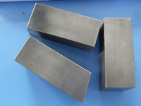
Rare tungsten has been widely used in the field of sputter deposition of semiconductor integrated circuits, solar photovoltaics, etc. due to its advantages such as high melting point, high strength, low thermal expansion coefficient, low resistivity, and good thermal stability. Tungsten targets are used mainly in the semiconductor field as diffusion barriers for integrated circuits and memory electrodes for large scale integrated circuits.
Semiconductor integrated circuits have high requirements on the purity of the target. Generally, the purity of the target must be above 99.999%. At the same time, the compactness of the target material also has an important influence on the coating process and the performance of the film layer. The compactness of the target material not only affects the deposition rate during sputtering, the density of the sputtered film particles, and the discharge phenomenon, but also affects the sputtering. Film electrical and optical properties. The denser the target, the lower the density of the sputtered film particles, the weaker the discharge phenomenon, and the better the performance of the thin film. Correspondingly, the melting point of tungsten is high, and we adopt the traditional powder metallurgy method. Although the finished product can be fired, the quality and performance are not stable, and it is difficult to fire a large-sized tungsten target.
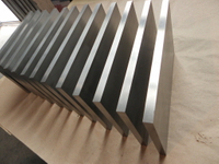
As the chip industry is the commanding point of high technology, it is an important strategic field. The target is also a necessary equipment for chip manufacturing. With the rapid development of semiconductor technology, the degree of integration is getting higher and higher, and the single crystal silicon chip integrator is per unit area. The number of pieces has grown exponentially, and the size of mainstream silicon wafers has gradually grown from 12 inches (300 mm) to 18 inches (450 mm). Therefore, how to manufacture larger-sized and high-quality tungsten targets has become a hot spot for the smelting of tungsten products.
In recent years, under the inspiration of the talents of countries such as the “Thousand Talents Program” and “Millions of People Plan”, a group of excellent teams have returned to China to start their own businesses and have been supported by major national science and technology projects such as “863” and “02 Special Projects”. After breaking the monopoly and blockade between Japan and the United States, after 12 years of arduous pioneering, it has established a production base based on a full range of domestically produced equipment and has complete independent intellectual property rights. There are talents, funds, and support from national policies. In this environment, China's high-purity metal refining technology has also achieved rapid development. Innovations in R&D have resulted in many patents with independent property rights. Chinese companies can already use them. Its own advanced production process produces tungsten target products no less than Japan-US companies, and many production bases such as tungsten hexafluoride and other special gases are gradually put into production. A new industrial chain is turning to manufacturing in China. Change some of the past high-tech materials can only rely on imports.
At present, China has built the world's largest integrated circuit target manufacturing line. Most of the supporting industries have been basically completed, and a full range of products has been produced in volume, supplying more than 280 chip manufacturing plants worldwide. The production of ultra-pure metal sputtering targets has an impurity element content of less than one in 100,000. It is used in the world's leading 10- to 28-nanometer technology very large-scale integrated circuit chip manufacturing. In the harvest season, Huawei has been able to design and With the manufacture of Chinese-advanced and advanced smart phone chips, Ziguang can create DDR4 memory chips that break the world's technological oligopolistic monopoly. No country dares to despise China's position in the large-scale integrated circuit industry.